Curator's Take
AI Commentary
This article matters because FBH’s new diamond‑processing service tackles one of the bottlenecks in scaling solid‑state quantum devices: producing high‑quality color‑center defects with repeatable optical and spin properties. By offering wafer‑scale fabrication that integrates precise ion implantation, annealing and surface treatment, the company bridges recent laboratory breakthroughs—such as record‑long coherence times for NV and SiV centers—and the need for manufacturable components in quantum sensing and communication hardware. If the process delivers consistent defect yields, it could accelerate commercial prototypes of diamond‑based quantum memories and magnetometers, though long‑term stability and integration with existing photonic platforms will still need to be demonstrated.
— Mark Eatherly
Summary
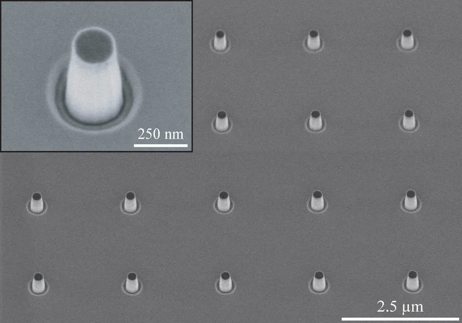
Insider Brief PRESS RELEASE — Diamond is attracting growing interest for quantum technologies. Defects in its crystal lattice, known as color centers, can behave like individual atoms. Their discrete spin states can be addressed through optical transitions, making them promising building blocks for quantum memories and light sources for quantum communication and sensing. Translating these […]